
My original effort on this topic is here, at #336. Do read that first, from October last year.
My takeaway from all of this is more enthusiasm, especially if you might be persuaded to fund some research, but actually this seems to me to be bogging down in process detail that academia is not actually helping progress much. We need reliably pure graphene; we need ways of maintaining that purity and we need reliable ways of processing it into the products we think we want. But we are not discovering what those things are because it is such a wonderful material that is acquires additions (such as additional atoms sticking within the net) which are, as yet, contaminants.
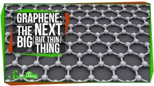
The images imply never-ending sheets of graphene, where the actuality to date are accurately called flakes. I'd like to see a calculation that shows what size of flake would be required to, say, match an existing recognised chip in magnitude.
I went looking for published updates from the scientific community and soon found [21] to [26].
Graphene’s incredible ability to conduct generated heat will result in less room needing to be taken up by thermal management mechanisms. Its superior radiation tolerance will make it invaluable in space-oriented applications, while a combination of its optical and conductive characteristics will be pivotal in the advancement of photonics — allowing faster modulation and higher degrees of sensitivity.
Key to graphene securing adoption within this sector will be the capacity for its production to be successfully aligned with established semiconductor fabrication processes. Looking at the development of integrated chips, the ideal would be for manufacturers of integrated circuits to find a way of utilising much of their existing plant to generate circuits with a graphene component. Currently, the commercial production of wide-area graphene monolayers relies on chemical deposition onto a metal catalyst (most commonly in the form of copper or nickel foil). If the graphene is going to be applied to a useful semiconductor substrate a transfer procedure needs to be carried out. This means etching away the copper film, picking up the graphene layer, and transferring it to a semiconductor wafer, like silicon. Copper from the catalyst that the graphene monolayer was originally grown on can end up being taken with it. The contamination impinging onto the graphene layer is detrimental to device reliability and yield. In addition, structural inconsistencies are commonly witnessed, which curb the performance parameters that can be achieved. The transfer process is labour intensive, which makes it not fit with existing processes and therefore adds to cost. As yet the lab processes have not proved scalable. Ideally, the graphene needs to be grown (deposited, perhaps) directly on the substrate. In my view, just being able to lead away the waste heat from a chip is an enormous improvement. That this same medium could simultaneously provide flexibility, structural strength and conductivity is still quite mind-blowing. That is why it is so disappointing that we are not making more immediate progress. It seems obvious to me that the early graphene-based devices will be more expensive than alternatives, but we need to see them in operation to realise what the true advantages may be. If the production issues can bring close to parity (say, less than twice the price) then it won't take long for more scalability to be discovered and Moore's law can resume its progress. [Doubling in some regard every two years].
[23] explains that silicon contamination is a likely cause of graphene promising much and delivering little. It is likely that it is the source material that is already contaminated, suggesting (to me) that some pre-processing to significantly lower contamination is a necessary process, almost no matter how expensive.
This also reported here and here and here.
[24] describes perhaps how to remove the contaminants. Abstract: Chemical vapour deposition (CVD) is among the most utilised techniques to fabricate single-layer graphene on a large substrate. However, the substrate is limited to very few transition metals like copper. On the other hand, many applications involving graphene require technologically relevant substrates like semiconductors and metal oxide, and therefore, a subsequent process is often needed to transfer CVD to the new substrate. As graphene is fragile, a supporting material such as a polymer film, is introduced during the transfer process. This brings unexpected challenges, the biggest of which is the complete removal of this support material without contaminating graphene. Numerous methods have been developed, each having advantages and drawbacks. This review will first introduce the classic transfer method using poly(methyl methacrylate) (PMMA) as the support material. The operating procedure and issues of PMMA residuals will be discussed. Methods to minimise/eliminate contamination will be presented, together with alternative approaches that do not require the use of PMMA. I tried reading a lot of this and I think that the issue is that decent quality graphene—and very high quality graphene is what is needed—has a very high surface energy, which means that anything / everything around is trying to stick to it, and that too easily includes contaminants which then lodge within the surface. It struck me, reading the content, that sufficient heat would drive off many contaminants. It is clear that this research needs to continue; the need for consistently (very) clean graphene is an essential for acquiring the benefits graphene offers. Since we want, almost immediately, to multiply up layers of graphene, we really need this process to be remarkably successful.
It is obvious that a 2-D material such as graphene is mostly surface (what is not surface is the width of an atom). Past research by me on painting metal structures suggests that the available surface at atom level might be three times (how I'd love that to be π) bigger than one thinks, but I don't see that as relevant; what matters is that other atoms can lodge in the gaps within the graphene matrix and (obviously, since this is what the research has shown), other materials readily stick to any available surface. Would that be van der Waals force attraction between layers? How would you calculate the expected change in density? Is there an early practical limit to packing such a surface? Might it be that an added atom is not so much in the surface as on it? Might that depend also on size and what else might 'stick' to such a surface (viruses?)?
So there are two issues here. One is to start with very high purity of graphite and the other is to find a process that keeps the graphene clean (pure) until it is coated with whatever become the preferred and deliberate materials.
[25] explains (some of) the issues in attempting to purify graphite. The monetary value of graphite depends largely on carbon content and flake size. Good, relevant content. The degree of heat required to purify graphite (starting from petroleum coke of coal tar pitch, 2500-3000ºC) is sufficiently high to 'motivate' natural graphite sources, found successfully in China, India, Brazil, Canada and Russia, all large countries. For those with far better Chemistry than me, Purification of graphite is its physical separation from an ore mixture. This process can be explained by the thermodynamic principle of ΔGM = ΔHM − TΔSM, in which GM, HM and SM are Gibbs free energy, enthalpy, and entropy of mixing at temperature T, respectively. Except for the stability condition of ΔGM < 0 and the second partial differential of ΔGM wrt xᵢ ( xᵢ is a mole fraction of component i), the spontaneous phase separation occurs. Accordingly, for effective separation or mixing, we may control the intermolecular interactions at the interfaces among each hydrophobic/hydrophilic or amphiphilic components. I lost it at the first equation, I'm afraid.
I liked §5.9: The processes such as microwave irradiation, leaching and filtering with acid (e.g., HCl and HNO3) could enhance the grade of graphite to more than 99%.
End conclusions included this, which, I think, says the usual; 'watch this space, more funds/research/investment needed':
So in order to stock sufficient graphite, both the deposit assessment at natural graphite exploration sites coupled with compatible purification methods affording ppm level of impurities in graphite are required. The technique for the purification of graphite from its gangue and trace elements depends on the estimated liberated size of the flake on the rock body. Specifically, size distribution would give an essential effect to overall process designs. In this regard, the well-established automated mineralogy [§5.3], with a mineral liberation analyzer (MLA) is highly encouraged. Practically, researchers and manufacturers of natural graphite are recommended to focus on both the pre-comminution separation method for efficient mineral liberation and the precise process design for further purification. Importantly, further intensive researches for minimizing the energy, time, and cost of production, as well as for developing the eco-friendly techniques of purification are still needed, which could be carried out based on the processing-structure-property-performance relationship from materials science point of view. While many countries in the world are well-known as natural graphite deposit-owning and mining countries, the economic significance of the deposit is not sufficiently studied, indicating the available future works for mineralogists.
I was left wondering if the assumption of starting from a carbon-rich ore is commercially valid, that maybe starting from somewhere else entirely, like ash, and then applying careful chemistry, might be a viable solution to the required purity. Maybe the significant leap occurs when the carbon is persuaded to form flat molecules which are then persuaded to polymerise into sheets. I then wondered if that described some already known plastics.
A long overview paper, [26] starts from an assumed pretty pure and certainly consistent graphene. A difficult read. My takeaway is that there's a lot of work being done, that it is difficult and, until someone has a marked success (and shares that) we're not much nearer actually turning graphene into the basis of the next chip. Quite simply, we can't produce it in enough volume to get on with finding out what it can be persuaded to do. We can see what ought to be possible, but we don't have enough of it of any consistent performance. And, when I say 'it', there are already many forms and I do not think we have yet discovered enough to know which forms would be worthy of extended exploration. As a breakthrough, the discovery of graphene continues to point to some sort of elysian field, but one still off in the distance. If the required leap in understanding is still ten years away then this is not going to be the route to salvation for which we are seeking. I can see funding sources soon looking elsewhere for the Next Big Thing.
Research paper style, we need more time (and funding, research, etc., etc.).
The New New Thing is a readable Michael Lewis book which I think relevant. But then I've read it; you may disagree; you may be of the opinion that anything even ten years old (the book was 1999) is so dated it couldn't possibly have relevance to today's world.
DJS 20220112
[21] https://www.sciencedaily.com/releases/2022/01/220106152433.htm
[22] https://www.eetimes.com/charting-graphenes-progress/#
[23] https://hexus.net/tech/news/industry/124946-research-reveals-reason-disappointing-graphene-progress/
[24] https://par.nsf.gov/servlets/purl/10147756
[25] https://www.sciencedirect.com/science/article/pii/S2095268618304269
[26] https://iopscience.iop.org/article/10.1088/2053-1583/ab1e0a
Additional Notes copied from #336.
I'm hoping someone with a better understanding will read, unravel and write to me.
The intention to rewrite last para., turned into sub-page to #380
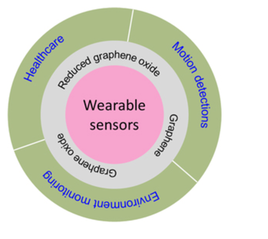
Clear confusion in media between graphene (expensive) and graphene oxide (relatively cheap). [13] First we must establish what is graphene or graphite. It is generally accepted that 2D sheets that are less than 10 layers thick can be called graphene. There are 3 main types of graphene: Graphene films which are typically made by CVD, ALD, or Epitaxial growth, Graphene Oxide which is exfoliated by reacting graphite in sulphuric acid with potassium permanganate in a highly exothermic reaction, & Graphene Nanoplatelets which can be plasma exfoliated or chemically exfoliated, ball milled, or thermally shocked and sheared to product stacks of graphene nanoplatelets. How to choose between graphene and graphene oxide? It depends on your application. If you want electronic properties to make a sensor or device or improved mechanical properties, we recommend CVD graphene, or RGO. If you want good dispersion and solution processing, we recommend normal GO.
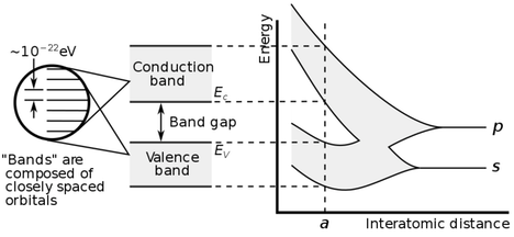
Not understood: the use of band and band-gap in chip design. This applies to semiconductors; a band gap, also called an energy gap, is an energy range in a solid where no electronic states can exist. In graphs of the electronic band structure of solids, the band gap generally refers to the energy difference (in electron volts) between the top of the valence band and the bottom of the conduction band in insulators and semiconductors. It is the energy required to promote a valence electronbound to an atom to become a conduction electron, which is free to move within the crystal lattice and serve as a charge carrier to conduct electric current. It is closely related to the HOMO/LUMO gap in chemistry. If the valence band is completely full and the conduction band is completely empty, then electrons cannot move in the solid; however, if some electrons transfer from the valence to the conduction band, then current can flow (see carrier generation and recombination). Therefore, the band gap is a major factor determining the electrical conductivity of a solid. Substances with large band gaps are generally insulators, those with smaller band gaps are semiconductors, while conductors either have very small band gaps or none, because the valence and conduction bands overlap. How chemistry (and solid-state physics) has moved since I was at school; this makes me feel utterly out of touch and I want a source that introduces these ideas in a sensible order. The diagram helped me, and led me to ask about interatomic distances in the different forms of carbon. The a shown is for diamond at about 0.357nm, while for graphite that figure is around 0.246nm. In graphene, 0,142nm and 0.335 between layers in the 3-d form. (researchgate and wikipedia).
Question: if conduction applies to electricity (and heat)?, what does rising energy with smaller interatomic distance mean? Does it mean that there is increased electron mobility [in graphene (15,000, 0.246) over graphite (250,000 0.142) say]. Does that also mean everything is hotter? [No, not necessarily]
Conventional semiconductors like silicon have a bandgap in the range of 1 - 1.5 electronvolt (eV), whereas wide-bandgap materials have bandgaps in the range of 2 - 4 eV. Generally, wide-bandgap semiconductors have electronic properties which fall in between those of conventional semiconductors and insulators. Wikipedia
Look up 'fitness patch',
Graphene oxide [GO] is a single-atomic layered material, made by the powerful oxidation of graphite, which is cheap and abundant. Graphene oxide is an oxidized form of graphene, laced with oxygen-containing groups. It is considered easy to process since it is dispersible in water (and other solvents), and it can even be used to make graphene. Graphene oxide is not a good conductor, but processes exist to augment its properties. It is commonly sold in powder form, dispersed, or as a coating on substrates.
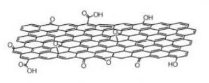
Graphene oxide is synthesised using four basic methods: Staudenmaier, Hofmann, Brodie and Hummers. Many variations of these methods exist, with improvements constantly being explored to achieve better results and cheaper processes. The effectiveness of an oxidation process is often evaluated by the carbon/oxygen ratios of the graphene oxide.
Graphene Oxide films can be deposited on essentially any substrate, and later converted into a conductor. This is why GO is especially fit for use in the production of transparent conductive films, like the ones used for flexible electronics, solar cells, chemical sensors and more. GO is even studied as a tin-oxide (ITO) replacement in batteries and touch screens.
Graphene Oxide has a high surface area, and so it can be fit for use as electrode material for batteries, capacitors and solar cells. Graphene Oxide is cheaper and easier to manufacture than graphene, and so may enter mass production and use sooner.
GO can easily be mixed with different polymers and other materials, and enhance properties of composite materials like tensile strength, elasticity, conductivity and more. In solid form, Graphene Oxide flakes attach one to another to form thin and stable flat structures that can be folded, wrinkled, and stretched. Such Graphene Oxide structures can be used for applications like hydrogen storage, ion conductors and nanofiltration membranes.
Then there is reduced graphene oxide, rGO [12]
Fast batteries - Huawei 2016, HowTo
Would bags of graphene decay? Does graphene decay at all? Could graphene displace plastic well or badly? What about embedding graphene in structure such as concrete, which could conduct heat away (to some useful place like a heat pump power generator), or provide heating and at the same time move electric power around.
How does price of graphene affect the possibilities? Since it is appearing in wearables, that implies its cost is already not preventatively expensive. Factors attaching to cost, at about $100 per gramme. Target has to be under $1/g. Graphene oxide is alrady less expensive, $75-225/g source
How are the medical applications working out? Even [11] is pretty quiet about this. Graphene contact lens?
Cars? Look at the Briggs (UK). Video sample.
Wearable tickets - printed electronics - internet of things effect. Article. (diagram too) [15]
DJS 20210127
[1] https://en.wikipedia.org/wiki/History_of_graphene. I think we will be taught that this occurred at Manchester University in 2003, earning 2010 Nobel prizes for Andre Geim and Konstantin Novoselov, who were both knighted in 2012. Geim has also produced gecko tape, which looks to suggest that Spiderman may become a reality.
[2] https://www.aps.org/publications/apsnews/200910/physicshistory.cfm
[3] https://www.photonicsviews.com/a-new-ultra-high-speed-terahertz-chip/ the latest fast chip I found.
[4] IBM says they've built a graphene chip. https://www.dcncorp.com/news/ibm_graphene-chip-faster-using-standard-cmos-processes/ Also https://www.extremetech.com/extreme/175727-ibm-builds-graphene-chip-thats-10000-times-faster-using-standard-cmos-processes?goback=%2Egde_2245236_member_5837731363922411524 A short, easy read. Original article: https://www.nature.com/articles/ncomms4086 One can envision that high-performance graphene RF circuits will be directly built on top of high-density Si CMOS logic circuits to form an extremely low-cost, ultra-compact communication system.
[5] https://www.chemistryworld.com/news/post-silicon-age-dawns-as-carbon-nanotube-transistors-made-in-chip-factories/4011927.article CNT transistors; roll graphene tightly and a band gap forms (?) so that it does behave like a semiconductor. This is often described as using nanotubes to make transistors.
[6] https://www.discovermagazine.com/the-sciences/move-over-graphene-next-gen-2d-materials-could-revolutionize-technology discusses other single layer atomic skins (my phrase). Hence: phosphorene, which has many qualities in common with graphene though it behaves more easily as a semiconductor and does odd things with light at infra-red wavelengths suggesting a future in fibre comms and solar cells; Borophene is very flexible, transparent, electrically conductive and a similar layer of boron nitride is a good insulator, so sandwiches of BN-B-BN have possibilities; chromium triiodide, CrI₃, generates a magnetic field and again needs to be sandwiched between layers of BN to be usable – the magnetic effect suggests possible uses in computing memory and storage. There's a future for physicists in atomically thin sheets, atomic skins. Triiodide, a rare occurrence of a doubled letter-i. Though at the end, as in leylandii, is not so unusual. Skiing, taxiing, grafitiing, shanghaiing, foliicolous, zombiisms.
[7] https://iopscience.iop.org/article/10.1149/2162-8777/abbb6f A good source, achieving what I wanted to know.
Graphene [has] better physical properties [when] compared to other materials, such as high thermal conductivity (5000 Wm−1 K−1),7 high electron mobility (250,000 cm2V−1 s−1),8 high Young modulus values (1.0 TPa),9large surface area (2630 m2 g−1),10 and better electrical conductivity and optical transmittance.11 I found this meaningless until I looked up the physical constants (how do you do that these days, I used to have a wonderful book of Father's that did this);
Thermal conductivity: aluminium 237 copper 401, diamond 1000 graphene 5000Wm⁻¹K⁻¹ wikipedia.
Electron mobility: GaN 800, crystalline silicon 1400, graphite 15000 (source), carbon nanotubes, 79000, graphene 250,000 cm²V⁻¹s⁻¹ wikipedia When I hunted further on that 250000 figure I found that is theoretical (Chen et al, 2008). See here, article by BM Nichols, 2D Materials, 2016, but that electronmobility of 70,000 cm²V⁻¹s⁻¹ was achieved at room temperatures. Almost readable.
Young's modulus (approx): brass 100, wrought iron and steel 200, tungsten carbide 550, graphene 1000, diamond 1100 GPa. wikipedia
Large surface area (specific surface area): alumina as catalytic support 200, fine clay montmorillonite 800, Faujesite catalyst 900, activated carbon 500-3000, graphene 2630, metal organic framework 7140 m²g⁻¹ wikipedia
Electrical conductivity (Ohm-metres x 10⁻⁹) graphene (by volume) 12, silver 16, copper 17, Gold 24 Look. Confused.
Optical transmittance: this depends on the wavelength of the light under consideration. graphene (presumably looking to see if it will replace phone screens and like uses). single layer graphene showed a transmittance of 97.49% at 550 nm wavelength, Optical glass transmits light well (over 99%) from about 375-1275 nm (visible light is 380-700nm; Infra-red is 780-1000 The infrared spectrum can itself be divided into three distinct categories: near-infrared or NIR (wavelength: 0.75 – 1.4 micrometers), short wavelength infrared or SWIR (wavelength: 1.4 – 3 micrometers), mid wavelength infrared or MWIR (wavelength: 3 – 8 micrometers), long wavelength infrared or LWIR (8 – 15 micrometers), and far-infrared or FIR (wavelength: 15 – 1000 micrometers). I'm sorry, that is not three but five bands. Messy topic, but one might ask what range certain sorts of sensor work in. Source... PIR detectors...
[8] https://en.wikipedia.org/wiki/Potential_applications_of_graphene Read after writing. I omitted the solar cells; I assumed that price would fall to competitive levels with other materials. Article gives good coverage (but what would I know; I call it good because it looked further than I did). How permeable to water is graphene? Could it make a light bulb?
[9] https://web.archive.org/web/20130320001240/http://bucky-central.me.utexas.edu/RuoffsPDFs/179.pdf on graphene-based ultra capacitors. The surface area of a single graphene sheet is 2630 m2/g, substantially higher than values derived from BET surface area measurements of activated carbons used in current electrochemical double layer capacitors. Our group has pioneered a new carbon material that we call chemically modified graphene (CMG). CMG materials are made from 1-atom thick sheets of carbon, functionalized as needed, and here we demonstrate in an ultracapacitor cell their performance. Specific capacitances of 135 and 99 F/g in aqueous and organic electrolytes, respectively, have been measured. In addition, high electrical conductivity gives these materials consistently good performance over a wide range of voltage scan rates. These encouraging results illustrate the exciting potential for high performance, electrical energy storage devices based on this new class of carbon material.
[10] https://www.graphene.manchester.ac.uk/learn/applications/ links to several other pages. Among these, that graphene oxide—a different material from graphene—can be used as membranes (between fluids). How about graphene packaging? Graphene water filters? Gas separators? desalination? If all that, how about inside batteries, where a membrane is often wanted between the electrodes?
[11] https://www.techradar.com/uk/news/dummy-40-ways-graphene-is-about-to-change-your-life
[12] Graphene-info https://www.graphene-info.com/ All you wanted to know (they think). Example, air purifiers (refers to germs, not viruses) https://youtu.be/p9IMn_uTv2Q
[13] https://www.cheaptubes.com/product-category/graphene-oxide/
[14] https://www.sciencedirect.com/topics/engineering/graphene Science gobbledegook mostly. The test is that if you can read material like this, it is okay for you. If you can't, the implication is that you shouldn't even be trying. I resent that. I tried reading the whole, some of which was actually interesting: Thin flakes of graphite were repeatedly peeled off the mesas using scotch tape. Then, we selected those flakes that were so thin as to remain practically invisible under an optical microscope. They were released by dissolving scotch’s visco-elastic layer in acetone and captured on a Si wafer. Large flakes often appeared crumpled. [....] We emphasise that despite many steps involved in the film and device microfabrication, the described procedures were found to be highly reproducible, except for the peeling-off process that in the end relies on manual selection of a most suitable thin flake.
[15] https://iopscience.iop.org/article/10.1149/1945-7111/ab67a4 Review—Wearable Graphene Devices for Sensing. Variably readable; images interesting.